Xuan Zhang, Mustansir Mukadam, and Ishita Mukhopadhyay
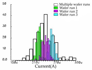
With technology scaling, circuit engineers face tremendous challenges in designing robust circuits. Among all the circuit-design challenges posed by deep sub-micron technologies (tolerating process variations, managing power budgets, meeting performance goals and overcoming short-channel effects), tolerance to process variations is emerging as the most important one. The histogram showed in Figure 1 illustrates how transistor output current may vary across multiple wafer runs, which is a vivid example of process variation. This is especially true for analog circuits; on-die and wafer-scale variations in transistors can result in a number of problems including unpredictable bias conditions, band width, skew, VCO frequency and tuning range. These challenges call for a design-stage statistical analysis and a systematic design methodology to achieve maximum yield.
 As a step in this direction, we propose a bottom-up approach towards process-invariant circuit design. Starting at the sub-circuit level, we have built various basic circuit blocks that have significantly-reduced process, supply voltage, and temperature sensitivity:
Current Source
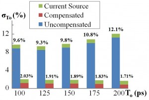
We have developed a promising design methodology based on device-level correlation to reduce the effect of intrinsic process variations without the need for post-fabrication efforts. Based upon this methodology, We have designed and optimized an example current source circuit, and measured it to have more than a factor of 2 improvement in normalized standard deviation over equivalent uncompensated current sources. The scaling behavior of the process-invariant current source in future technology nodes is found to remain unchanged despite the worsening process variability of single transistors at smaller technology nodes.
Frequency Reference
 Responsible for generating the “heart-beat” of the system, the frequency reference can “make-or-break” the whole system, and its variability will directly affect the overall yield. We have investigated the application of both open-loop and closed-loop feedback in process compensation with low variation ring oscillator. The carefully-designed compensation schemes are able to reduce the variation in the center frequency by more than 80%, meaning a factor of 5 improvement. They show great potential to confine the standard deviation of center frequency within 1%, making possible a fully-integrated self-calibrated self-adjusted stable frequency generator for application in microcontrollers and wireless sensor networks.
Low Noise Amplifier
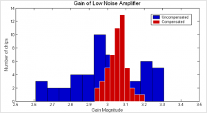
 Low Noise Amplifiers (LNA)- the first active block in a receiver chain – have to be extremely robust to variations in process, temperature, and supply voltage, to maintain the receiver’s noise and intermodulation specifications. We focus on designing process compensating circuit blocks to minimize the variation in the gain of an LNA with the help of statistical feedback mechanisms. The circuits we have designed in the TSMC 65nm process are successfully able to reduce the variation in gain of conventional LNA systems by over 70%.
Data Converter
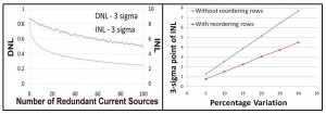
 Digital-to-analog converters (DAC) for calibration purposes need to be highly accurate. But due to process variations, the accuracy of these DACs is affected. The differential nonlinearity (DNL) and the integral nonlinearity (INL) are two of the parameters to measure the accuracy of the DACs. There are 3 types of current steering DACs-thermometer coded, binary coded and segmented, which is a mix of the thermometer and binary. The thermometer coded DACs are most accurate at the expense of area. It has been shown that adding redundancy helps in reducing the DNL and the INL and thus improving the accuracy. Another method to reduce the INL in thermometer coded DAC is reordering the way the current sources are switched on and added to the output current.
Our next step is to come up with more building blocks with low variation, and hopefully to set up a whole tool kit for analog circuit design.